Latest Version
Version
12.0
12.0
Update
December 05, 2024
December 05, 2024
Developer
Engineering Wale Baba
Engineering Wale Baba
Categories
Education
Education
Platforms
Android
Android
Downloads
0
0
License
Free
Free
Package Name
engg.hub.ad.semiconductor.device
engg.hub.ad.semiconductor.device
Report
Report a Problem
Report a Problem
More About Semiconductor Device & Circuit
This Semiconductor Devices & Circuits App is designed for quick learning, revisions, references at the time of exams and interviews.
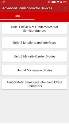
This Semiconductor Device App has160 topics with detailed notes, diagrams, equations, formulas & course material, the topics are listed in 5 chapters. The app is must have for all the engineering science students.
Semiconductor devices are nothing but electronic components that exploit the electronic properties of semiconductor materials, like as silicon, germanium, and gallium arsenide, as well as organic semiconductors.
This app cover most of related topics and Detailed explanation with all the basics topics.
Some of the topics Covered in the Engineering eBook are:
1. The Haynes-Shockley Experiment
2. Semiconductor Materials
3. Crystal Lattice
4. Cubic Lattices
5. Planes and Directions
6. The Diamond Lattice
7. Bulk Crystal Growth
8. Growth of Single Crystal Ingots
9. Wafers
10. Epitaxial growth
11. Vapor-phase epitaxy
12. Molecular beam epitaxy
13. Charge Carriers in Semiconductors
14. Effective Mass
15. Intrinsic Material
16. Extrinsic Material
17. Electrons and Holes in Quantum Wells
18. The Fermi Level
19. Compensation and Space Charge Neutrality
20. Drift and Resistance
21. Optical absorption
22. Photoluminescence
23. Electroluminescence
24. Carrier Lifetime and Photoconductivity
25. Direct Recombination of Electrons and Holes
26. Indirect Recombination; Trapping
27. Steady State Carrier Generation; Quasi-Fermi Levels
28. Photoconductive Devices
29. Diffusion Processes
30. Diffusion and Drift of Carriers: Built-in Fields
31. Diffusion and Recombination; The Continuity Equation
32. Steady State Carrier Injection: Diffusion Length
33. Gradients in the Quasi-Fermi Levels
34. Temperature Dependence of Carrier Concentrations
35. Effects of Temperature and Doping on Mobility
36. High-Field Effects
37. The Hall Effect
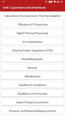
38. Fabrication of p-n Junctions: Thermal oxidation
39. Diffusion of P-N junction
40. Rapid Thermal Processing
41. Ion Implantation
42. Chemical Vapor Deposition (CVD)
43. Photolithography
44. Etching
45. Metallization
46. Equilibrium Conditions
47. Equilibrium Fermi Levels
48. Space Charge at a Junction
49. Forward- and Reverse-Biased Junctions
50. Carrier Injection
51. Reverse Bias
52. Reverse-Bias Breakdown
53. Zener Breakdown
54. Avalanche Breakdown
55. Rectifiers
56. The Breakdown Diode
57. Transient and A-C Conditions
58. Reverse Recovery Transient
59. The Ideal Diode Model
60. Effects of Contact Potential on Carrier Injection
61. Switching Diodes
62. Capacitance of p-n junctions
63. Recombination and Generation in the Transition Region
64. Ohmic Losses
65. Graded Junctions
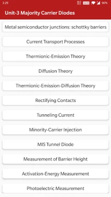
66. Metal semiconductor junctions: schottky barriers
67. Current Transport Processes
68. Thermionic-Emission Theory
69. Diffusion Theory
70. Thermionic-Emission-Diffusion Theory
71. Rectifying Contacts
72. Tunneling Current
73. Minority-Carrier Injection
74. MIS Tunnel Diode
75. Measurement of Barrier Height
76. Activation-Energy Measurement
77. Photoelectric Measurement
78. Ohmic Contacts
All topics are not listed because of character limitations.
Each topic is complete with diagrams, equations and other forms of graphical representations for better learning and quick understanding.
Features :
* Chapter wise complete Topics
* Rich UI Layout
* Comfortable Read Mode
* Important Exam Topics
* Very simple User Interface
* Cover Most Of Topics
* One click get related All Book
* Mobile Optimized Content
* Mobile Optimized Images
This app will useful for quick reference. The revision of all concepts can be finished within Several hour using this app.
Instead of giving us a lower rating, please mail us your queries, issues and give us valuable Rating And Suggestion So we can consider it for Future Updates. We will be happy to solve them for you.
Rate the App
Add Comment & Review
User Reviews
Based on 0 reviews
No reviews added yet.
Comments will not be approved to be posted if they are SPAM, abusive, off-topic, use profanity, contain a personal attack, or promote hate of any kind.
More »


Popular Apps

MouserMouser Electronics, Inc.

ALLDATASHEET - Datasheet PDFInterbird Co., Ltd

Hidden Objects GamesMorion Studio

American TallAmerican Tall LTD

My Town: Police Games for kidsMy Town Games Ltd

Find It - Hidden Object GamesGuru Puzzle Game

ESGCT CongressLumina-EU

Prison Life: Idle GameSupercent, Inc.

ASGCT EventsAmerican Society of Gene & Cell Therapy

Talkspace Therapy & CounselingTalkspace
More »


Editor's Choice

Voyage FCUVoyage Federal Credit Union

Todoist: Planner & CalendarDoist Inc.

Zoho ProjectsZoho Corporation
ClockGoogle LLC

Adventure Escape MysteriesHaiku Games

Sky MapSky Map Devs

GUESS 81GUESS?, Inc.

TALL Embark -Language LearningGlobal Educational Technologies

American TallAmerican Tall LTD

Dinosaur Police Car kids GamesYateland - Learning Games For Kids
